


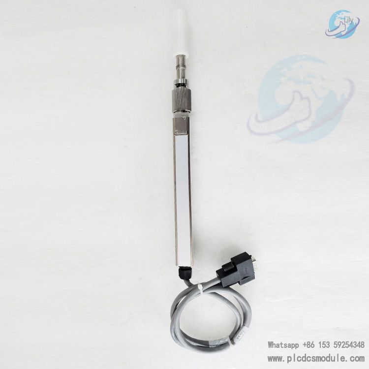
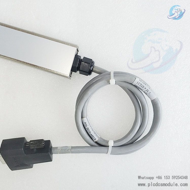
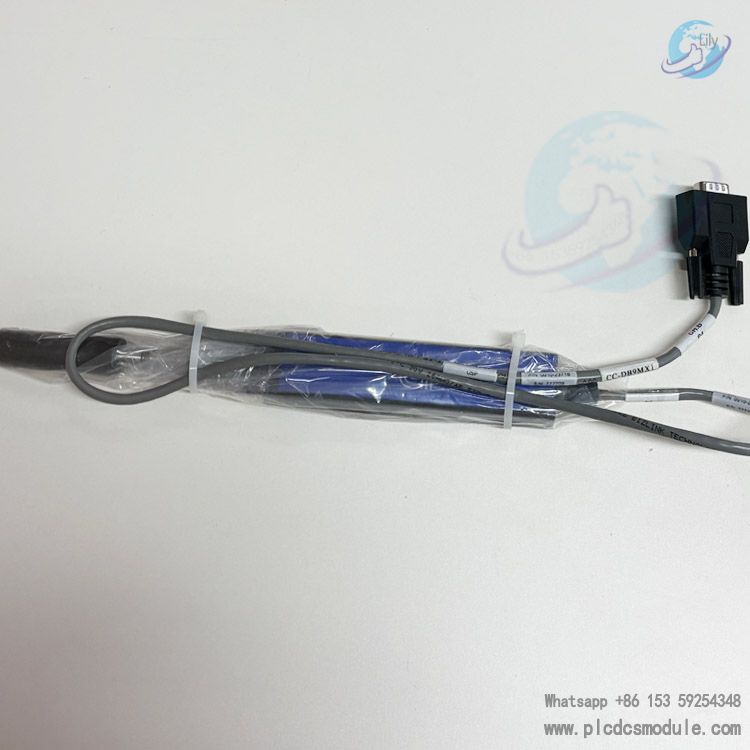
The 0010-44213 emitter is a device component of AMAT (Applied Materials) used in specific processes within semiconductor manufacturing, display technology and other fields.
In the field of semiconductor manufacturing, AMAT emitters are used in key process steps such as plasma etching and chemical vapor deposition (CVD). For example, in plasma etching, the emitter is responsible for generating and emitting plasma. Composed of ions, electrons, and neutral particles, plasma can undergo physical and chemical reactions with the surface of semiconductor materials to achieve precise etching of the materials, thereby creating complex circuit patterns on silicon wafers. In the chemical vapor deposition process, the emitter may be used to accurately control the injection and distribution of reaction gases. It uniformly emits gaseous precursor materials into the reaction chamber, where these precursors undergo chemical reactions on the surface of silicon wafers to deposit various thin films, such as metal films and oxide films, which are important steps in constructing the structure of semiconductor devices.
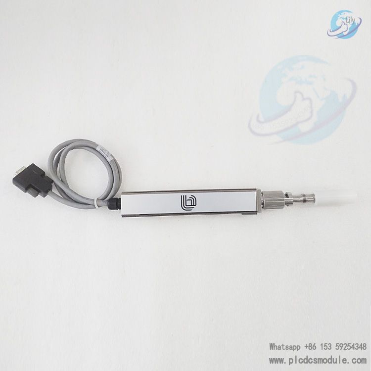
Other potential fields: Applied Materials has a wide range of businesses. In addition to semiconductor and display technology fields, it also involves industries such as solar photovoltaics and data storage. In the manufacturing process of solar cells, the AMAT 0010-44213 emitter is used to emit ions or photons, participating in processes such as silicon wafer doping and surface treatment to improve the photoelectric conversion efficiency of solar cells.
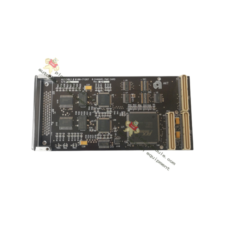
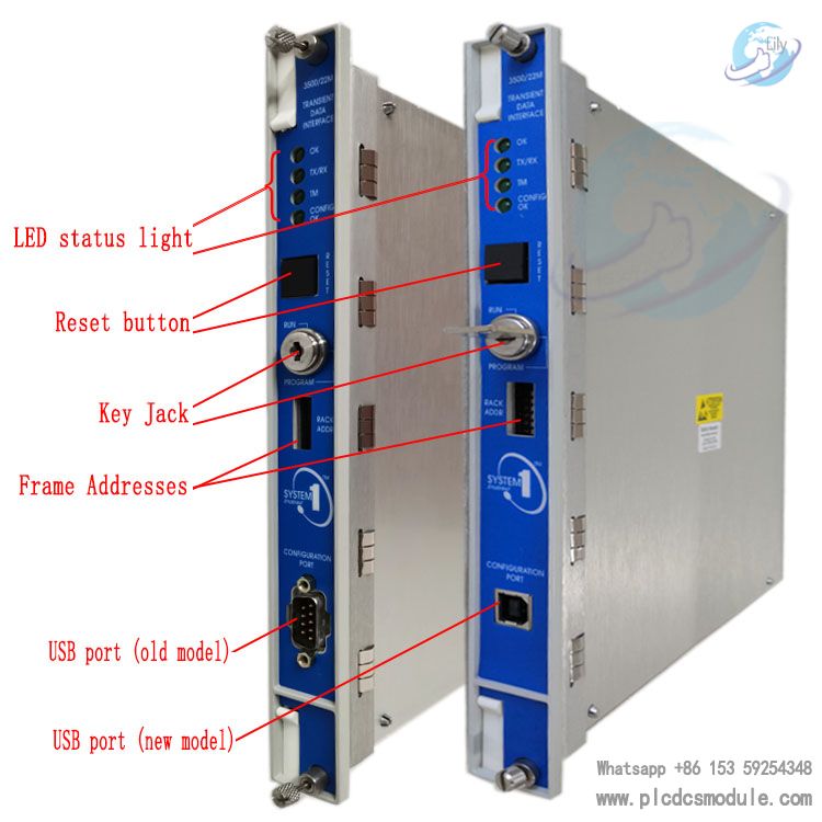
Customers who purchased this product are also browsing the following products:
AMAT 0010-23715 PMAX Emissometer
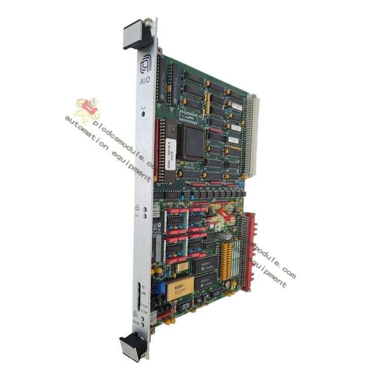
AMAT ASSY 0190-15384 I/O Board DELTA TAU CPCI 603603-106 32-Input 16-Output
SCHNEIDER 140ACO13000 Analogue output modules
National Instruments SCXI-1338 CURRENT INPUT, HIGH-VOLTAGE TERMINAL BLOCK
FOXBORO FDC280 RH101FQ Field Device Controller


 3005319639