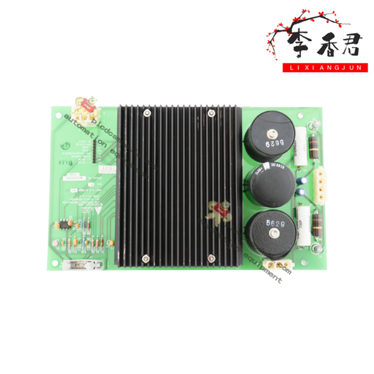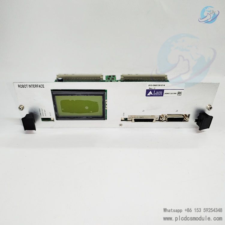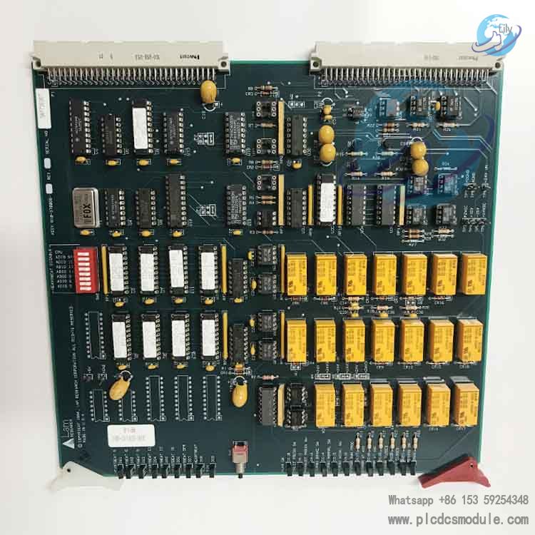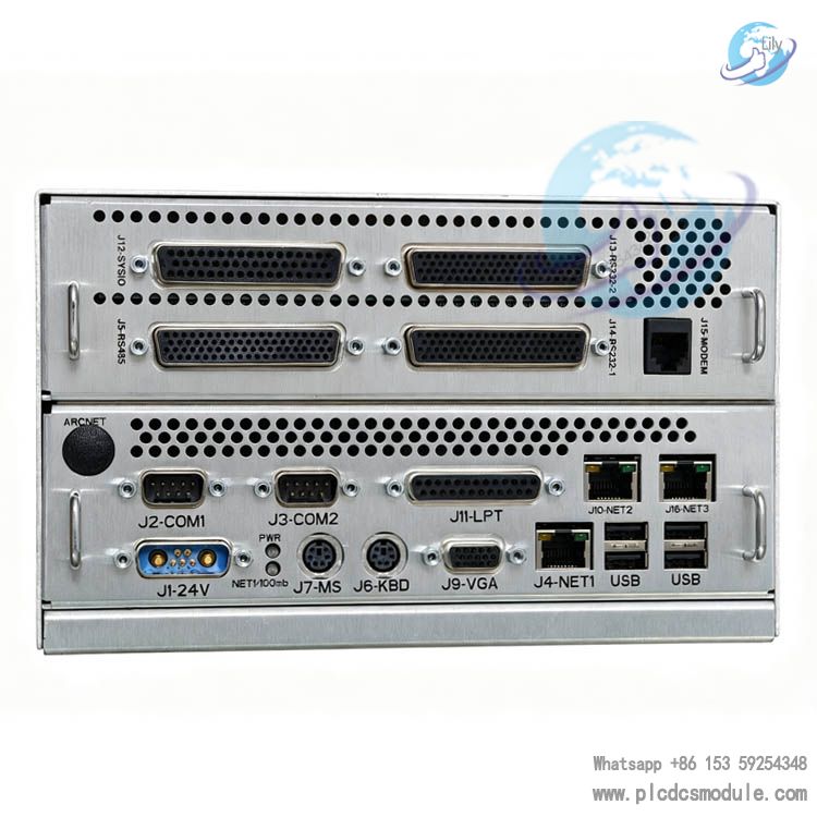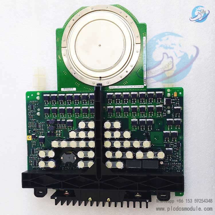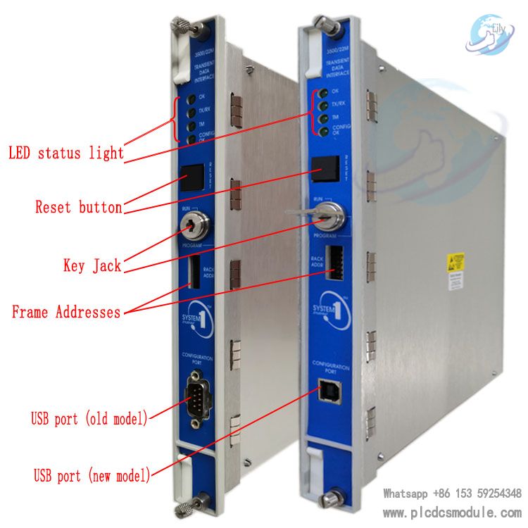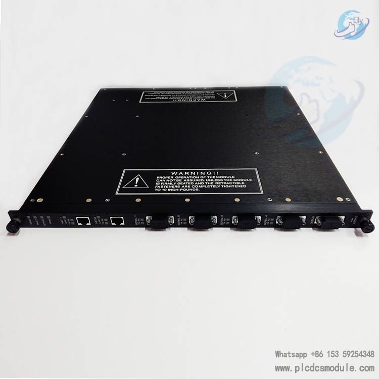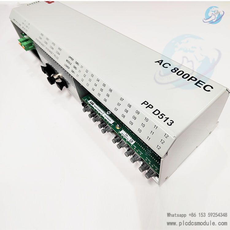


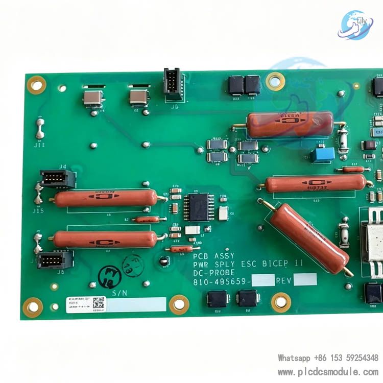
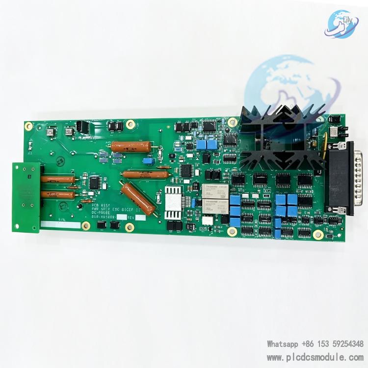
Lam Research 810-495659-307 is a dedicated power supply PCB for BICEP electrostatic chuck, belonging to Lam Research 810-series ESC power board product line. It acts as a core power control component for 300mm plasma etch systems. This board delivers high-precision adjustable high voltage output to electrostatic chucks for wafer clamping, and performs real-time voltage & current sampling with closed-loop voltage regulation. It ensures uniform wafer clamping force, preventing wafer shift, wafer drop, abnormal etch profile and other process defects. It is fully compatible with continuous mass production environment of cleanroom BICEP dual-chamber etch platforms.
Technical Features
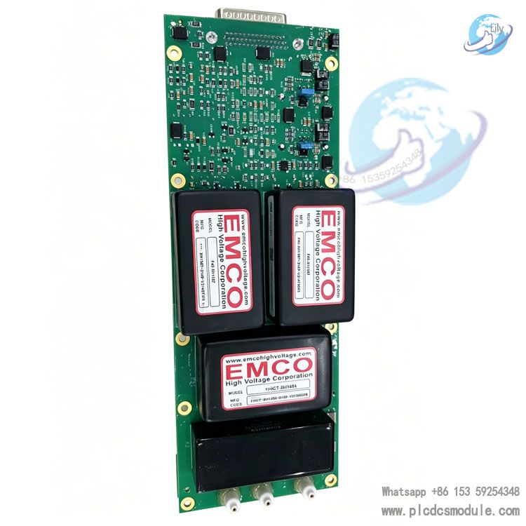
- Dual-channel high-voltage output architecture with embedded industrial EMCO high voltage conversion modules. The output voltage can be linearly adjusted, with voltage fluctuation limited within ±0.3%, supporting seamless switching of positive and negative bias for electrostatic chucks.
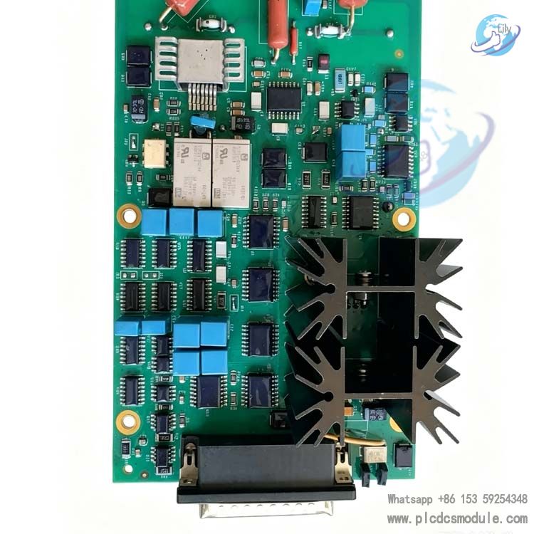
- Full-link electrical protection circuits integrated, including overvoltage, overcurrent, overtemperature, short-circuit and reverse polarity protection. It cuts off high voltage output within milliseconds upon abnormal load conditions to protect ESC, chamber and overall control system.
- Multi-layer PCB with impedance-matched routing and independent shielding layers to suppress RF interference generated by plasma chambers, maintaining high precision signal sampling under strong electromagnetic environment of etch equipment.
- Modular card-cage design with standard VME slot form factor, supporting tool-free rapid disassembly and installation. On-board debug port allows engineers to read operating parameters independently during maintenance, improving fault localization efficiency by over 60%.
- Industrial wide-temperature range components adopted, operating ambient temperature ranging from 18℃ to 70℃, complying with Class 1 semiconductor cleanroom temperature & humidity standards, supporting 7×24h non-stop continuous operation.
Model Decoding
Full part number: 810-495659-307
- 810: Main category prefix for Lam Research PCB assemblies, used to distinguish power supply boards, IO boards, motion control boards and RF control hardware.
- 495659: Base material code, fixed identifier for base PCB layout of BICEP platform ESC power mother board. Hardware circuit and high voltage module layout remain identical for all variants sharing this base code.
- 307: Revision suffix, numeric code representing hardware revision. 303, 307 and 511 are mainstream iterations of this base layout. Differences between suffix numbers lie in pinout definition, underlying firmware logic and fine-tuning of output power. Revision 307 features optimized high voltage ripple suppression circuit to meet high uniformity process requirements for advanced technology nodes
Product Characteristics
- Power Control Characteristic: Dual-polarity high voltage output with seamless positive-negative voltage switching. Output current is regulated via closed-loop real-time adjustment, automatically matching output power based on wafer size and process type.
- Signal Interaction Characteristic: Dedicated backplane communication bus enables real-time data exchange between the power board and equipment main CPU. Voltage, current, temperature and fault alarm signals are synchronously uploaded to equipment HMI terminal.
- Hardware Durability Characteristic: Conformal coating applied on board surface to resist trace corrosive process gas and moisture inside cleanrooms, extending board service life.
- Compatibility Characteristic: Exclusively compatible with Lam Research BICEP-series etch chamber platforms. Hardware interchangeability exists between revision 303, 307 and 511 of the same base code, only requiring matching equipment firmware version.
- Diagnostic Characteristic: On-board storage chip automatically records 30-day operating logs and fault alarm history. Maintenance staff can export logs via debug port to quickly identify intermittent electrical failures.
Application Fields
- Semiconductor Logic Chip Fabrication: Matching 7nm-28nm 300mm wafer dry plasma etch processes, FinFET transistor structure etch, providing stable clamping for ultra-thin large-size wafers.
- Memory Chip Manufacturing: Etch processes for 3D NAND multi-layer stack structures and DRAM wafers. It eliminates wafer displacement during multi-layer dielectric etch and improves full-wafer etch uniformity.
- Advanced Packaging Process: Supporting TSV through-silicon via etch and fan-out packaging wafer processing equipment, compatible with low-temperature etch conditions for thin carrier wafers.
- Semiconductor Foundry Production Lines: Standardized BICEP dual-chamber mass production cluster etch equipment for 12-inch wafer high-throughput continuous manufacturing factories.
Working Principle
External 24V DC industrial power is transmitted to this power supply PCB through equipment backplane. Embedded EMCO high voltage conversion modules convert low input voltage to adjustable high voltage, which is delivered to electrostatic chuck electrodes via multi-channel output cable harness.On-board high-precision sampling circuits continuously collect real-time voltage and current signals at output terminals, which are transmitted to on-board FPGA control chip. FPGA compares process voltage parameters issued by equipment main controller and dynamically adjusts output power of high voltage modules to form closed-loop voltage regulation, maintaining constant ESC wafer clamping force.Integrated temperature sensors monitor operating temperature of PCB and high voltage modules simultaneously. If voltage, current or temperature exceeds safe threshold, on-board protection circuit immediately cuts off high voltage output, uploads fault code to equipment main controller via backplane bus and triggers equipment audio-visual alarm to lock chamber process programs and prevent process accidents.When equipment process recipes switch between wafer clamp and release actions, main controller sends voltage polarity switching commands to FPGA, which rapidly switches output polarity of high voltage modules to complete cyclic wafer clamping and releasing operations.
Cross-series Product Comparison
| Comparison Item | 810-495659-307 | 810-495659-303 | 810-495659-511 | 810-107813-105 |
|---|---|---|---|---|
| Compatible Platform | BICEP Dual-chamber Etch Platform | BICEP Dual-chamber Etch Platform | BICEP Dual-chamber Etch Platform | Single-chamber ESC Power Platform |
| High Voltage Ripple Suppression | Optimized multi-stage filter circuit, ultra-low ripple | Basic filter circuit, medium ripple | Enhanced overcurrent protection, medium ripple | Single-channel output, general ripple control |
| Output Channel Quantity | Dual high voltage output channels | Dual high voltage output channels | Dual high voltage output channels | Single high voltage output channel |
| Hardware Interchangeability | Hardware interchangeable with 303/511, firmware matching required | Hardware interchangeable with 307/511 | Hardware interchangeable with 303/307 | Not interchangeable with above three models |
| Applicable Technology Node | Advanced 7-28nm Logic & Memory Chips | Mature nodes above 28nm | Thick wafer processes requiring high current | 8-inch mature process single-chamber equipment |
| Core Optimization Focus | Reduce RF interference, improve voltage stability | Standard mass production base version | Strengthen short-circuit protection for thick wafers | Low-cost matching for compact single-chamber equipment |
FAQ
Q1: Can revision 810-495659-307 directly replace revision 303 during installation?A1: Hardware interface and slot dimension are fully identical, PCB can be directly inserted into card cage. After replacement, corresponding revision firmware must be matched in equipment background system, otherwise error codes for unrecognized voltage output parameters will appear.
Q2: How to distinguish quality differences between brand new, refurbished and dismantled used PCB during procurement?A2: Brand new PCB comes with complete factory anti-static packaging and factory electrical test report, conformal coating remains intact without scratches. Refurbished PCB has replaced aging components and re-sprayed conformal coating with shorter warranty period. Dismantled used PCB is spare part disassembled from retired equipment with accumulated operation loss, only suitable for temporary emergency backup.
Q3: PCB continuously reports overcurrent fault during operation, which components should be prioritized for inspection?A3: First inspect electrostatic chuck electrode insulation layer for damage and electric leakage, check high voltage output cable harness for damaged shielding layer and short circuit. Secondly inspect aging failure of internal EMCO high voltage modules on PCB. Finally check short-circuit issues caused by corrosive process gas erosion on chamber electrodes.
Q4: How many electrostatic chucks can a single 810-495659-307 power board drive simultaneously?A4: This model adopts dual-channel output design. One single PCB can drive two independent electrostatic chucks of dual chambers on BICEP platform synchronously, voltage and current parameters of two output channels can be adjusted separately.
Q5: For bulk procurement of multiple identical PCB units, is individual on-machine debugging required for every single unit?A5: Brand new unused PCB has passed standardized factory electrical inspection. Only 10% sample units need on-machine verification after bulk purchase. Refurbished and dismantled used PCB must undergo complete no-load and full-load on-machine debugging for each unit to eliminate hidden electrical faults.
Q6: PCB stored for long-term idle without operation, what pre-processing operations are required before re-installation?A6: Take PCB out of anti-static packaging bag and place inside cleanroom constant-temperature environment for 24-hour static balance. Power on PCB under no-load condition for 30 minutes preheating, test high/low voltage output of dual channels sequentially. Export built-in PCB operation log and confirm no storage faults before connecting electrostatic chuck load.
Q7: What practical production-level improvements does revision 307 deliver compared with revision 303?A7: Revision 307 adds multi-stage RF filter circuits. When high-power RF generators of etch chambers are activated, voltage fluctuation of high voltage output is reduced by 70%. During ultra-thin 12-inch wafer clamping processes, uniformity of clamping force at wafer edge is improved, lowering volume of defective wafers caused by edge etch irregularities.
Q8: What is the standard routine maintenance cycle for this power supply PCB, and what items are included in maintenance procedures?A8: Standard maintenance cycle for mass production fab lines is 6 months. Maintenance procedures include cutting off power supply then cleaning dust accumulated on PCB surface, inspecting oxidation and wear conditions of high voltage cable harness connectors, exporting operation logs to analyze long-term voltage fluctuation data, performing full-range voltage performance retest under no-load mode, replacing aging components in advance if abnormal performance is detected.
Cross-series Model Recommendation
- 810-495659-303, BICEP ESC Power Supply Board
- 810-495659-511, BICEP ESC High Voltage Power PCB
- 810-107813-105, Single Chamber ESC Power Supply Board
- 810-225831-001, Equipment Power Driver PCB
- 810-141736-005, Process Signal Interface Board
- 810-069751-114, Etch Chamber Control PCB
- 810-099175R013, RF Signal Processing PCB
- 810-240284-005, Equipment IO Signal Acquisition Board
- 810-800156-002, Multi-channel Analog Control Board
- 605-017016-100, Stepper Motor Driver Control Board
- 605-017034-004, VME Bus CPU Main Control Board
- 685-069171-100, Plasma Process Coordination Control Module
- 210-70305-00, Process Fault Alarm Signal PCB
- 660-327289-402, Equipment Mainframe DC Power Supply Unit